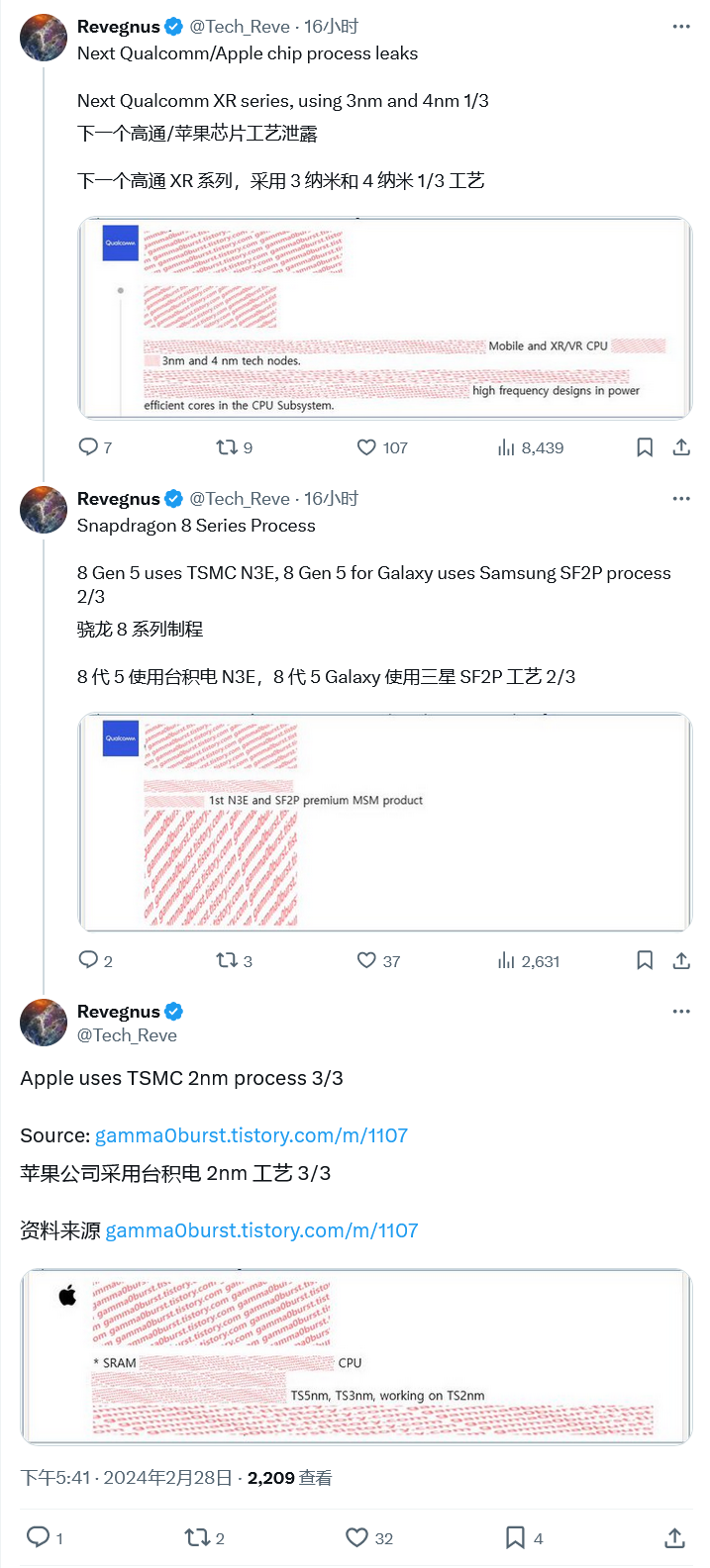
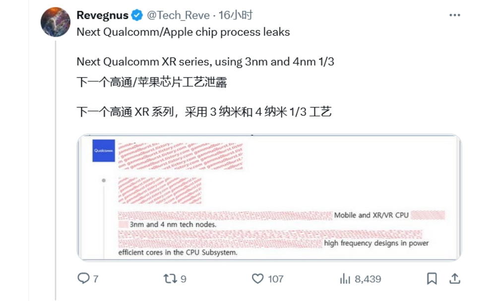
Igeekphone on February 29 news, news source @Tech_Reve recently tweeted that including the Snapdragon 8 Gen 4 released this year, all Qualcomm’s flagship chips are fully manufactured using TSMC’s 3nm process, but the Snapdragon 8 Gen 5 launched next year will adopt a multi-fab program.
The report said Samsung produced the Qualcomm Snapdragon 8 Gen 1 chip, due to overheating and inefficiency, Qualcomm turned to TSMC, which has since become its exclusive contract manufacturing partner.

This pattern will change next year, in which the regular Snapdragon 8 Gen 5 chips continue to be manufactured by TSMC’s 3nm process N3E, while the Snapdragon 8 Gen 5 chips for Samsung’s flagship Galaxy S26 series use Samsung’s SF2P process.
Note: Compared to SF3, the SF2 process can improve power efficiency by 25% for the same frequency and complexity, improve performance by 12% for the same power and complexity, and reduce area by 5% for the same performance and complexity.
To make the SF2 process more competitive, Samsung will also offer a range of advanced IP combinations for the process, including LPDDR5x, HBM3P, PCIe Gen6 and 112G SerDes, among others.
SF2P is optimized for high-performance computing (HPC) based on the SF2 process, and is expected to have greater improvements in performance.
Previous news said that Qualcomm Snapdragon 8 Gen 5 will use the “Pegasus” core, using the “2+6” cluster design scheme and Slice GPU architecture.


